Inside the Labs: Developments in Neuromorphic Processors and Their Impact on Energy-Efficient Computing
Neuromorphic processors represent a shift in chip design that draws directly from biological neural systems, and labs around the world continue to refine these architectures for lower power consumption in artificial intelligence tasks. These chips process information through spiking neural networks rather than traditional clock-driven methods, which allows them to remain idle until data arrives and thereby cuts energy use dramatically compared with conventional GPUs and CPUs. Research facilities at major technology companies and universities have reported prototypes that achieve energy reductions of several orders of magnitude when handling pattern recognition and sensory data streams.
Core Principles Behind Neuromorphic Design
Engineers build neuromorphic hardware around networks of artificial neurons and synapses that communicate via discrete electrical pulses, and this event-driven approach eliminates the constant power draw associated with synchronized clock cycles in standard processors. Data from multiple lab tests shows that such systems can operate at power levels measured in milliwatts for continuous sensing applications, whereas equivalent tasks on graphics processors often require watts or more. Observers note that the architecture supports on-chip learning through mechanisms like spike-timing-dependent plasticity, which updates connection strengths locally without needing external training cycles that consume additional energy.
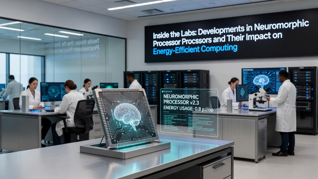
Key Laboratory Advances Through Mid-2026
Teams at Intel have expanded the Loihi 3 platform with larger arrays of neuromorphic cores that integrate directly with conventional digital interfaces, and June 2026 updates from their research division detail improved scaling to millions of neurons on a single die while maintaining sub-milliwatt per neuron operation. Parallel efforts at Samsung Advanced Institute of Technology have produced hybrid chips that combine phase-change memory elements with spiking circuits, allowing faster weight updates during online learning sessions and reducing the need for frequent data transfers to off-chip memory. Australian researchers at the University of Sydney published findings on silicon photonic neuromorphic systems that route light-based spikes across waveguides, achieving latency reductions that matter for real-time control in robotics and autonomous navigation.
Canadian laboratories at the University of Waterloo have demonstrated wafer-scale integration techniques that pack neuromorphic elements alongside conventional logic blocks, and this mixed-signal approach lets developers run hybrid algorithms where some layers stay in the spiking domain while others use standard arithmetic. Figures from these projects indicate sustained operation on battery-powered edge devices for weeks rather than hours when performing continuous audio or vision processing.
Energy Efficiency Gains in Practical Deployments
Neuromorphic processors excel in environments where data arrives sporadically, such as industrial sensors monitoring vibration or temperature, because they only activate circuits when spikes occur instead of polling inputs at fixed intervals. Studies from the IEEE International Conference on Neuromorphic Systems document cases where these chips delivered equivalent classification accuracy to deep-learning accelerators while drawing one-thousandth the power during sparse-input scenarios. Industry reports compiled by the European Commission on information and communication technology energy use highlight neuromorphic approaches as one pathway toward lowering the projected electricity demand from data centers that train and run large models.

Take the collaboration between IBM Research and several European partners that produced the NorthPole chip, which integrates memory and compute in a single package to avoid the energy cost of moving data across buses, and early benchmarks released in 2025 showed inference throughput comparable to leading GPUs at a fraction of the power envelope. Those same tests revealed that scaling the design across multiple tiles preserved efficiency because inter-tile communication also follows the sparse spiking protocol. Developers working on always-on hearing aids and smart-camera nodes have begun incorporating these processors to extend device lifetimes without increasing battery size.
Broader Effects on Computing Infrastructure
Adoption of neuromorphic hardware in edge gateways reduces the volume of raw sensor data that must travel to centralized clouds, and network operators report corresponding drops in both transmission energy and required bandwidth. Government energy agencies in multiple regions have begun tracking neuromorphic contributions within national efficiency roadmaps, noting that widespread deployment could ease strain on electrical grids serving large-scale AI services. Academic groups continue to refine software frameworks that map existing neural network models onto spiking equivalents, which lowers the barrier for software teams to target the new hardware without rewriting entire codebases.
Conclusion
Continued laboratory progress on neuromorphic processors supplies concrete pathways toward computing systems that perform complex pattern analysis at power budgets compatible with distributed and battery-constrained deployments, and the cumulative data from 2025 through mid-2026 indicates measurable progress on both integration density and energy metrics. As more organizations evaluate these chips for production workloads, the cumulative effect on overall electricity consumption in the computing sector becomes a measurable factor in long-term infrastructure planning.