23 May 2026
Mapping Electron Pathways in Next-Generation AI Chip Designs

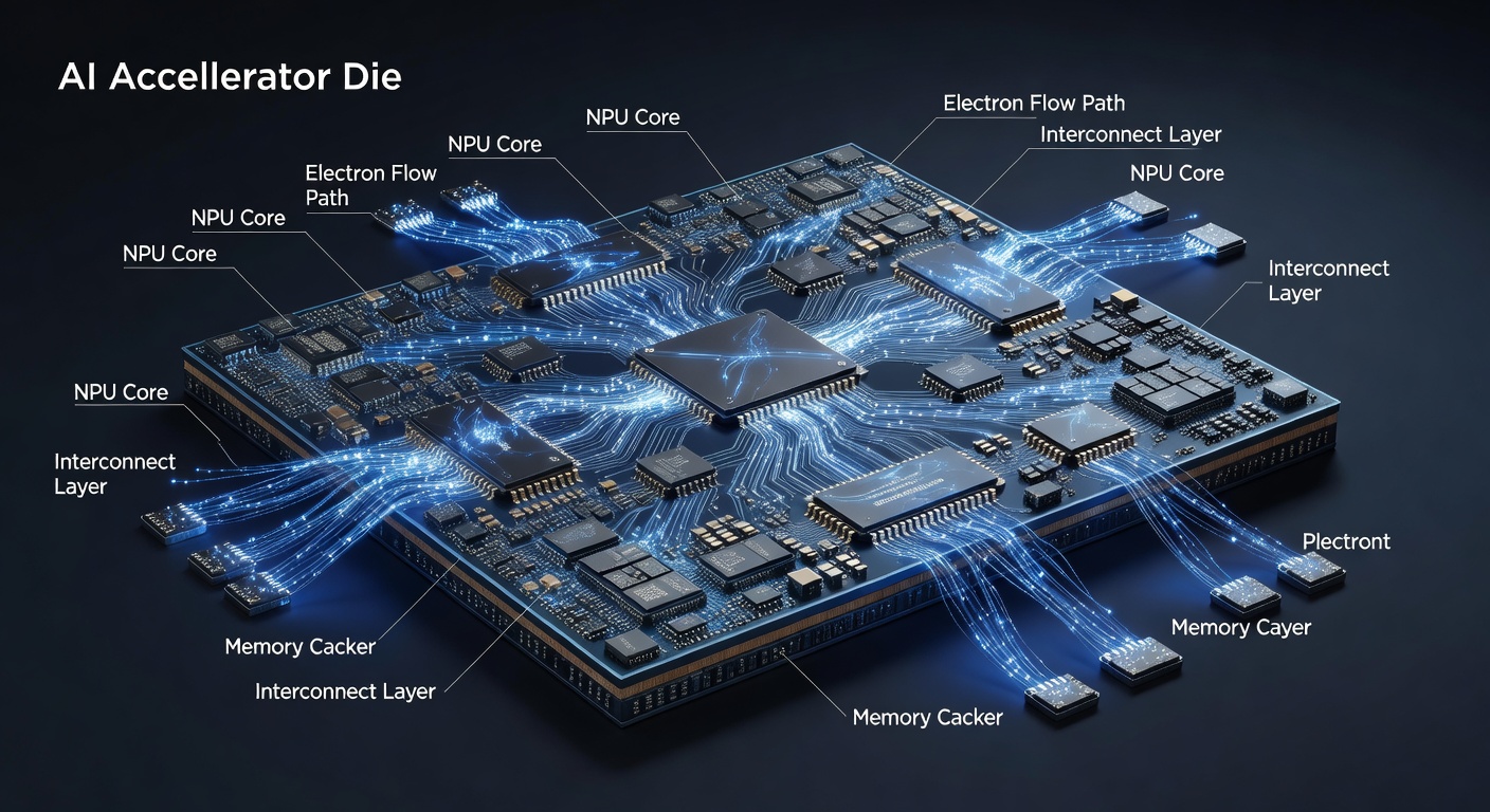
Advanced semiconductor architectures in AI accelerators rely on precise control of electron movement through complex transistor networks and interconnects, and researchers continue to develop new methods for tracing these flows as chip designs scale to smaller nodes. Data from industry analyses indicate that AI accelerators now incorporate billions of transistors where electron paths determine both performance and energy efficiency, while fabrication techniques push materials and geometries to their limits. Observers note that tracing these flows requires combining simulation tools with physical measurements because traditional probing methods fall short at nanoscale dimensions.
Fundamentals of Electron Movement in Modern Chips
Electrons travel through doped silicon regions, metal gates, and high-k dielectrics under applied voltages, yet scattering events and quantum effects alter their trajectories at each stage. Studies from semiconductor research centers show that in finFET and gate-all-around structures, carriers move in confined channels where mobility depends on crystal orientation and strain engineering. Those who've examined cross-sections of recent AI chips find that interconnect resistance and capacitance dominate power consumption once transistors switch at gigahertz frequencies, and mapping these interactions helps engineers optimize layout for lower latency in matrix multiplications central to neural network operations.
Techniques such as electron beam induced current imaging and scanning tunneling microscopy allow direct visualization of current paths, while time-resolved measurements capture transient behaviors during switching cycles. According to reports from the National Science Foundation, collaborations between academic labs and foundries have produced datasets that correlate electron density maps with device performance metrics, revealing hotspots where current crowding reduces reliability over time. And because AI workloads involve massive parallel computations, uniform electron distribution across processing elements becomes essential for sustained throughput.
Advanced Architectures and Tracing Challenges
Three-dimensional stacking and chiplet integration introduce vertical electron pathways that add complexity to flow analysis, since through-silicon vias must maintain low resistance while minimizing thermal gradients. Researchers at institutions across North America and Europe have documented how heterogeneous integration mixes logic dies with high-bandwidth memory stacks, creating mixed-signal environments where digital and analog electron behaviors interact in unexpected ways. What's interesting is that even minor variations in via alignment can shift current distribution enough to affect inference accuracy in trained models running on these accelerators.
Simulation frameworks based on drift-diffusion and Monte Carlo methods now incorporate machine learning to predict flow patterns across entire dies, cutting computation time while improving accuracy. Figures from TSMC technology roadmaps released ahead of 2026 production cycles reveal that 2-nanometer and beyond nodes will require atomic-scale precision in material deposition to control electron tunneling and leakage. People who've worked with these tools often discover that combining electrical test data with optical emission microscopy provides a more complete picture than either method alone, especially when identifying defects introduced during extreme ultraviolet lithography steps.
Developments Emerging in Mid-2026
By May 2026, several foundries had begun qualifying new metrology equipment designed specifically for real-time electron flow monitoring during wafer processing, and early adopters report tighter process control that reduces variation across AI accelerator batches. European research consortia have published joint findings on graphene-enhanced interconnects that alter electron transport characteristics, offering potential reductions in resistive losses for high-frequency operations. Industry organizations such as the Semiconductor Industry Association track these advances through quarterly reports that link material innovations directly to accelerator benchmarks in training and inference tasks.
One study revealed that integrating sensors within test chips allows continuous logging of local current densities, feeding data back into design iterations without destructive analysis. Observers note that regulatory frameworks from bodies like the U.S. Department of Commerce now emphasize supply chain traceability for critical semiconductor materials, indirectly supporting consistent electron behavior across global manufacturing sites. And because AI accelerators power data centers worldwide, improvements in flow tracing translate into measurable gains in overall system efficiency measured in teraflops per watt.
Applications and Measurement Integration
Practical deployment of these tracing methods extends to failure analysis teams who isolate marginal defects before they impact large-scale deployments, while design teams use the resulting models to refine placement of power delivery networks. Academic papers indexed in IEEE Xplore demonstrate how hybrid approaches merge finite element analysis with experimental validation, producing maps that guide layout adjustments for better thermal management alongside electrical performance. Those who've studied this know that accurate electron flow data also supports security evaluations, since side-channel leakage often correlates with localized current patterns during cryptographic operations embedded in AI edge devices.
Equipment vendors continue to refine probe technologies that operate at cryogenic temperatures to suppress thermal noise during measurements, enabling clearer signals from the smallest features. Data indicates that adoption rates for these advanced tools have risen steadily as AI accelerator volumes increase, driven by demand from hyperscale computing providers seeking predictable behavior under sustained loads. Researchers discovered that cross-referencing multiple tracing modalities yields higher confidence in identifying subtle process variations that single techniques might miss.
Conclusion
Tracing electron flows through advanced semiconductor architectures remains central to advancing AI accelerator performance, with ongoing refinements in measurement and simulation supporting continued scaling. Organizations and research groups from multiple regions contribute data that informs both fabrication practices and architectural choices, while emerging capabilities in 2026 point toward tighter integration of monitoring directly into production flows. The resulting insights help maintain reliability and efficiency as designs incorporate ever more complex three-dimensional features and novel materials.