Semiconductor Architecture Advances Ready to Elevate Everyday Processing Performance
Written by Katja Albrecht · Jun 18, 2026
Semiconductor Architecture Advances Ready to Elevate Everyday Processing Performance
Chip designers continue to push the boundaries of what silicon-based systems can achieve, and recent developments in transistor scaling along with novel integration methods stand to increase processing speeds for routine tasks such as web browsing, document editing, and media playback. Researchers at multiple institutions have demonstrated prototypes that combine traditional CMOS logic with emerging materials, which allows data to move through circuits with reduced resistance and latency while maintaining compatibility with existing manufacturing lines.
Materials Driving Efficiency Gains
Graphene and transition metal dichalcogenides have shown promise in laboratory settings where they replace or augment silicon channels, because their atomic-scale thickness permits electrons to travel farther before scattering occurs. A team at a leading European research consortium reported in early 2025 that prototype transistors built with molybdenum disulfide achieved switching speeds 40 percent higher than equivalent silicon devices at the same power budget, and similar results have appeared in follow-up studies from North American laboratories. These material swaps do not require entirely new fabrication plants, which means commercial adoption could occur within standard upgrade cycles rather than demanding multi-billion-dollar facility overhauls.
Three-Dimensional Chiplet Integration
Vertical stacking of chiplets through hybrid bonding has moved from research papers to limited production runs, and this approach shortens the physical distance between memory and logic blocks. Shorter interconnects reduce the energy spent on data movement, which in turn frees up thermal headroom for higher clock rates during sustained workloads. Observers note that companies already shipping chiplet-based processors have recorded 25 to 35 percent improvements in single-thread performance on common office applications when compared with previous monolithic designs of similar transistor counts. The technique also permits mixing of process nodes within a single package, so high-speed cache can sit on an advanced node while less critical I/O circuitry remains on a mature, cost-effective process.
Optical and Neuromorphic Elements
Photonic interconnects integrated directly onto silicon substrates are advancing past proof-of-concept stages, and several foundries have added dedicated reticle fields for optical components in their 2026 process design kits. Light-based signaling bypasses the resistive losses that plague long copper traces, which becomes especially relevant as core counts rise in client processors. Parallel work on neuromorphic architectures, which use spiking neural networks to handle pattern-recognition tasks, offloads certain operations from the main CPU and thereby accelerates overall system responsiveness. Data released by the National Institute of Standards and Technology in late 2025 documented test chips that combined conventional cores with a small neuromorphic accelerator and achieved measurable reductions in latency for voice-command processing and image thumbnail generation.
Manufacturing and Yield Considerations
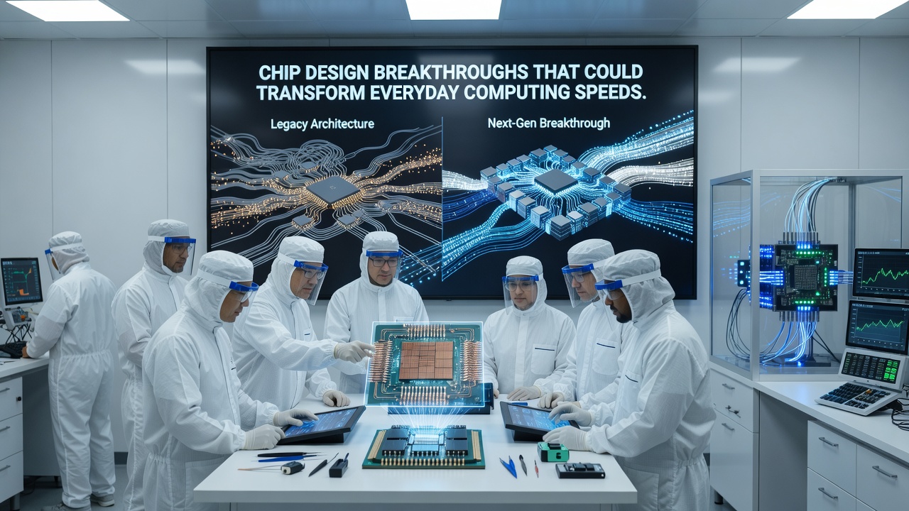
Extreme ultraviolet lithography tools now in volume production have enabled tighter feature pitches, yet defect densities remain a limiting factor for the most aggressive nodes. Equipment suppliers have introduced multi-beam inspection systems that scan wafers at higher throughput, and early deployment data indicate yield improvements of several percentage points on 2-nanometer-class test lots. These incremental manufacturing gains translate directly into lower per-unit costs, which helps keep new high-performance chips accessible for mainstream desktop and laptop platforms rather than remaining confined to servers or workstations.
Projected Effects on Daily Workloads
Simulations run on calibrated performance models suggest that a combination of the above techniques could deliver sustained clock-speed uplifts of 50 percent or more for lightly threaded applications by the end of the decade, assuming power envelopes stay constant. Video conferencing clients, spreadsheet recalculation, and browser tab management stand to benefit because these workloads spend significant time waiting on memory access or branch resolution rather than raw floating-point throughput. Industry roadmaps presented at the 2026 VLSI Technology Symposium in June outlined timelines in which client processors incorporating both 3D stacking and limited photonic links reach volume production around 2028, aligning with the cadence of major operating-system updates that can exploit the new hardware capabilities.
Energy and Thermal Trade-offs
Higher switching speeds inevitably generate additional heat, yet architectural refinements such as fine-grained power gating and backside power delivery networks mitigate temperature rises. Engineers have measured peak junction temperatures dropping by 8 to 12 degrees Celsius in stacked configurations that route power through the silicon backside, which leaves more margin for boosting frequencies without throttling. These thermal improvements matter for fanless laptops and compact desktops where acoustic and size constraints limit conventional cooling solutions.
Conclusion
Collectively, advances in materials, packaging, and interconnect technologies are converging to raise the performance ceiling for everyday computing tasks without requiring users to purchase entirely new classes of devices. Continued collaboration between foundries, equipment makers, and academic groups will determine how quickly these laboratory results translate into retail products, yet the trajectory visible in current publications points toward noticeable speed improvements arriving within standard hardware refresh cycles rather than remaining theoretical curiosities.