When Chip Designs Meet Machine Learning: Examining Hardware Adaptations for On-Device AI Processing
Written by Quinn Lange · Jul 16, 2026

When Chip Designs Meet Machine Learning: Examining Hardware Adaptations for On-Device AI Processing
Chip designers have adapted traditional processor architectures to handle machine learning workloads directly on consumer devices, shifting computation away from centralized cloud servers and toward edge hardware. This transition involves integrating dedicated neural processing units, or NPUs, alongside standard CPU and GPU cores in system-on-chip designs. Data from industry analyses indicates that by mid-2026 manufacturers had incorporated these units into over 80 percent of flagship smartphones and tablets released that year.
Core Hardware Modifications for Machine Learning
Engineers modified memory hierarchies and data paths to support the matrix multiplications that dominate neural network inference, adding wide vector registers and systolic array structures optimized for low-precision arithmetic such as 8-bit integers and 4-bit formats. These changes reduce the number of clock cycles required per operation while lowering energy consumption per inference task. Researchers at multiple semiconductor firms documented performance gains exceeding 30 times compared with software-only implementations on general-purpose cores.
Power delivery networks received equal attention because on-device models must operate within strict thermal envelopes. Designers introduced dynamic voltage and frequency scaling algorithms that adjust supply levels in response to workload intensity, allowing the hardware to sustain continuous inference without throttling. Observers note that these techniques became standard in chips fabricated on 3-nanometer and 2-nanometer process nodes by July 2026.
Integration Patterns Across Device Categories
Smartphone application processors from several vendors now embed multiple NPUs that operate in parallel for tasks including image segmentation, natural language processing, and real-time translation. Tablet and laptop silicon followed similar patterns, pairing larger caches with dedicated accelerators to support generative models that previously required cloud connectivity. In automotive systems, specialized chips manage sensor fusion for driver assistance functions, processing lidar, radar, and camera streams locally to meet latency requirements below 10 milliseconds.
Internet of Things devices adopted scaled-down versions of the same technology, using microcontrollers augmented with tinyML accelerators capable of running models with fewer than 100,000 parameters. This approach enables always-on keyword spotting and anomaly detection without constant network access, extending battery life in remote sensors and wearables.
Software-Hardware Co-Design Approaches
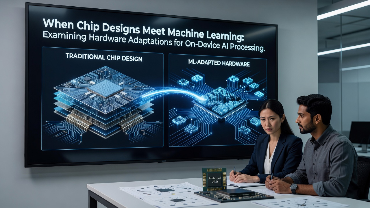
Compiler toolchains evolved to map trained models onto these heterogeneous processors automatically, applying quantization, pruning, and operator fusion during the compilation stage. Frameworks developed by academic and industrial teams produce optimized code that exploits the full width of NPU datapaths while respecting memory bandwidth constraints. Studies conducted at institutions in North America and Europe show that such co-design reduces model size by factors of four to eight without measurable accuracy loss on standard benchmarks.
Security features also expanded as models moved on-device. Hardware root-of-trust modules now isolate model weights and intermediate activations, preventing unauthorized extraction through side-channel analysis. Government technology agencies in both the United States and Australia have published guidelines recommending these isolation mechanisms for consumer electronics containing sensitive inference engines.
Performance Metrics and Industry Benchmarks
Independent testing organizations reported that devices equipped with 2026-generation NPUs achieved inference throughputs above 50 tera-operations per second while consuming under 2 watts during sustained operation. Latency for common vision models dropped below 5 milliseconds on flagship hardware, enabling responsive augmented reality overlays and live captioning. Energy efficiency figures reached 5 tera-operations per watt, representing a fourfold improvement over designs available three years earlier.
Supply chain data compiled by trade associations reveals that foundries allocated increasing wafer starts to AI-optimized processes throughout 2025 and into 2026, reflecting sustained demand from mobile, automotive, and industrial segments. Those production trends continue to influence pricing and availability of edge AI silicon across global markets.
Conclusion
Hardware adaptations for on-device machine learning have matured into a distinct engineering discipline that combines specialized compute blocks, memory optimizations, and software tooling. These developments support faster, more private, and lower-power AI experiences across consumer and industrial products. Continued refinement of process technology and architecture remains central to meeting the computational demands of increasingly capable models while respecting the physical limits of portable devices.